Inspection solutions
for advanced materials
NLOPTICS develops and markets non-destructive optical characterization tools dedicated to new advanced materials (GaN, LiNbO3, HfO2, SiC, …) and to the optimization of manufacturing processes in photonics and semiconductors.
Technological innovation at the service of your sectors of activity

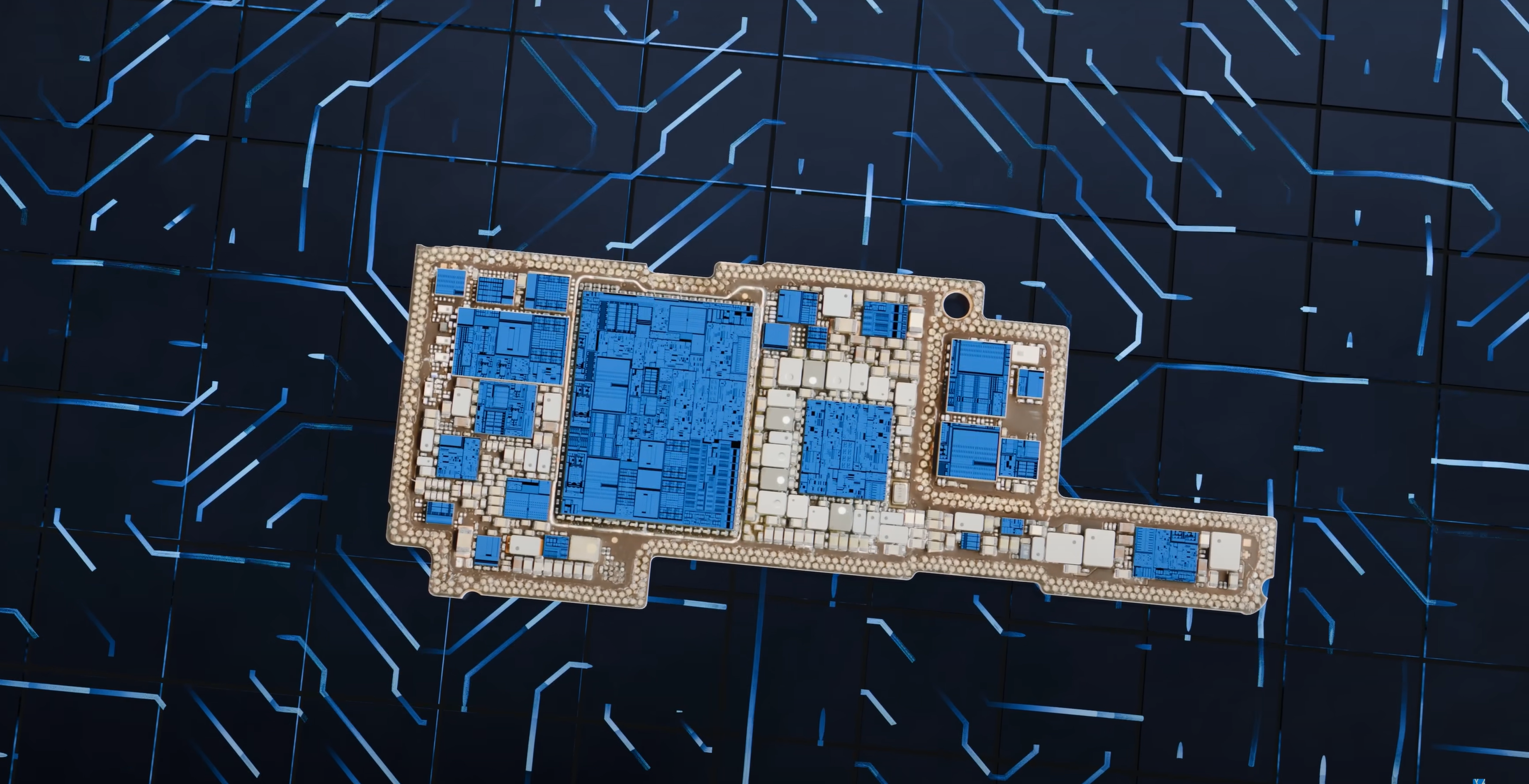
Integrated Photonics
Nonlinear optical coefficients evaluation
Optical axis determination
Electro-optic coefficients evaluation
Material engineering qualification (e.g.poling)
Degree of anisotropy assessment

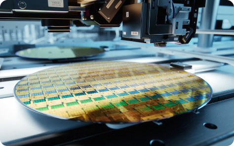
Semiconductors
Crystaline defects and phases characterization
Substrates quality assessment (dislocations)
Static charges imaging
Functional epitaxy monitoring
Within wafer uniformity deposition assessment
Why choose nonlinear optics?
Towards new manufacturing standards
The rise of AI, quantum computing, and 6G relies on a new generation of advanced materials that requires more stringent quality control than ever before.
At NLOPTICS, we are responding to this challenge with a nonlinear optical based technology that can reveal defects invisible to conventional methods, and support the industrialization of these strategic materials.
-
-
- Non-destructive and contactless : no alteration of samples, suitable for industrial processes in all circumstances.
- Compatibility with advanced materials : LiNbO3, GaN, HfO2, SiC, AlN, SiO2, InP, GaAs, Al2O3, diamond, glass, metals, and more.
- Direct access to functional properties : residual charges, degree of anisotropy, layer deposition homogeneity, crystal orientation.
- Surface and thin film analysis : can detect nanometer-thick depositions, ideal for critical interfaces and contaminant detection.
- Revealing the invisible : highlights defects, anomalies, and inhomogeneities that conventional optical methods cannot detect.
- Supporting innovation : accelerates the integration of next-generation materials in photonics and semiconductors.
-

Tools and analytical services designed around your industrial reality
Recognized expertise
At NLOPTICS, we continuously invest in R&D. Our goals are to improve our technologies, and expand the capabilities of our measuring devices.
We work closely with industrial and academic partners to remain at the forefront of innovation in non-destructive metrology.


Upcoming events
Meet us at our upcoming events to discover our tailor-made solutions
SEMICON Europa
18 - 21 November 2025 - Munich, DE
French Tech Day
27 November 2025 - Bordeaux, FR
Semaine de l'Innovation
28 November 2025 - Bordeaux, FR
SPIE Photonics West
20 - 22 January 2026 - San Francisco, USA
© 2026 – NLOPTICS. All rights reserved.
Terms of use
Privacy policy
Cookie policy